TECHNICAL SPECIFICATIONS
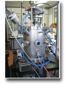
Home-made IONVAC HFCVD-01
-
Possibility of feeding single or multiple filaments (>10) with electrical power up to 7 kW to allow them to reach temperatures of about 2200-2400 ° C;
-
The positioning of filaments allows the homogeneous deposition of diamond layers on circular wafers up to 4" in diameter;
-
Operating pressures up to 100 mbar;
-
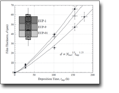
VBy varying the partial pressure and the precursor/hydrogen ratio, it's possible to obtain growth rates between 0.5e 5 μm/hr;
-
PAbility to independently heat the substrate up to 800°C;
-
Possibility of high vacuum heat treatments (P < 10-7 mbar);
-
3 Separate flow meters for H2 (300 sccm), Ar (50 sccm) e CH4 (10 sccm).
AVAILABLE TECHNIQUES
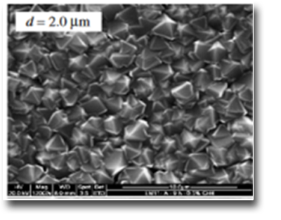
- deposition of poly and nano-crystalline diamond;
- heat treatments on large area samples, with temperatures up to 800 °C.
SAMPLES
-
Size of substrates up to 4 inches in diameter;
-
Polycrystalline diamond growth on the following substrates: silicon, refractory metals (molybdenum, tungsten, tantalum), carbides and nitrides;
-
Growth of nanodiamond coatings on a wide range of metals and semiconductors.
USED FOR
The use of diamond produced with HFCVD is recommended for:
- Thermal dissipation;
- Protective coatings of tools;
- Applications in electronic emission.
CASE STUDIES
The influence of grain-boundaries on the electronic performance of CVD diamond films
This scientific article shows the influence of grain boundaries on the electronic properties of the CVD diamond used as an X-ray detector. Several experimental tests show that the microstructure of the diamond film is composed of almost perfect crystalline grains, containing a very low density of defects, and grain boundaries. Such interfaces include flaws and non-diamond domains. The results show that substrate pretreatment is critical to control the initial grain nucleation density and thus the electronic performance of CVD diamond films.
See: Trucchi et al., Dia. Relat. Mater. 14 (2005) 575-57
Optimization of the performance of CVD diamond electron multipliers.s
This scientific article is focused on optimizing the properties of a CVD diamond converter to be used as an efficient backscattered electron (BSE) signal amplifier. The scope of application is in scanning electron microscopy (SEM) in order to allow an improvement in the contrast of the BSE image. A series of polycrystalline diamond samples was deposited with the HFCVD technique on previously treated silicon substrates, maintained at a temperature of 770 ° C. The material was produced with a [CH4] / [H2] concentration ratio of 0.5% and a total pressure of 12 Torr.
See: D. M. Trucchi et al., Dia. Relat. Mater. 15 (2006) 827-832.
 English (UK)
  Italiano (Italia)