2D-3D microfabrication with fs laser
coupled to a uFAB workstation
Stefano Orlando - stefano.orlando@ism.cnr.it
FemtoLAB in sharing with DiaTHEMA LAb
TECHNICAL SPECIFICATIONS
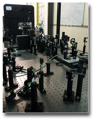
Spectra Physics Ti:Sa “fs” Laser
- Spitfire Pro - Regenerative Amplifier
- TEM00
- ʎ= 800 nm
- Emax = 4 mJ
- RepRate = 1kHz;
- timpulso = 120 fs;
- ʎSHG = 400 nm;
- Emax@400= 1.5 mJ
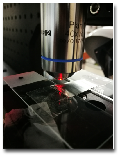
Newport uFAB Workstation
- Translation resolution: (x, y) 5 nm; (z) 20 nm;
- Magnification optics 4x, 20x, 40x
AVAILABLE TECHNIQUES
Use of single or double pulse configurations with time delays ranging from 100 fs to 2 ns
- Micro and nano-texturing of the surface of any material;
- microfabrication within the transparent solids
- creation of color centers in large band gap materials
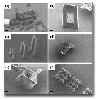
Scanning electron microscopy images of structures fabricated by 2-photon lithography. All the samples reveal the three-dimensional nature of the microstructures. The scale bars are 20 μm in (a), (c), (d), (e), and 10 μm in (b) and (f)
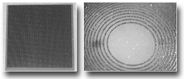
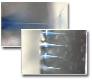
Optical microscopy images of 100 vertical graphitic walls embedded in a diamond plate (left) and a Fresnel lens for far-IR fabricated on a diamond plate surface (right)
SAMPLES
-
Max workable size:
-
Software limitation: 50 x 50 mm2 (x,y); 5 mm (z);
-
With manual positioning: 100 x 100 mm2 (x,y); 5 mm (z).
-
USED FOR
-
surface nanostructuring
-
surface graphitizations
-
internal graphitizations
-
creation of color centers
-
realization of microchannels in bulk materials
-
diffraction gratings
CASE STUDIES
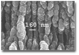
Surface nanostructuring to optimize the absorption of light in solar concentrators
The treatment with ultrashort pulse laser of diamond surfaces represents an innovative solution to increase the limited absorbance of the solar spectrum resulting from the wide bandgap of the diamond itself. This treatment is able to produce a material such as black diamond, introducing defects in the bandgap and nanostructuring the surface so as to effectively trap the photons of incident solar radiation.
See:
- FP7-Energy Collaborative - E2PHEST2US, Grant Agreement n.241270 (2010-2012)
- FP7-Energy FET - ProME3THE2US2, Grant Agreement n.308975 (2013-2016)
- H2020 FET-OPEN - AMADEUS, Grant Agreement n.737054 (2017-2020)
- Daniele M., Trucchi, Advanced Energy Materials 8, 1802310 (2018) DOI: 10.1002/aenm.201802310
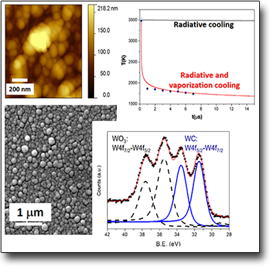
Creation of color centers in large gap materials (e.g. ionic crystals)
- Creation of conductive traces within insulating materials (eg graphite traces inside diamond);
- creation of micro-channels by self-focusing the laser beam using long focal length lenses (> >1 m).
See: Sergey M., Avanesyan, Appl. Surf. Sci. 248, 129 (2005)
DOI:10.1016/j.apsusc.2005.03.014
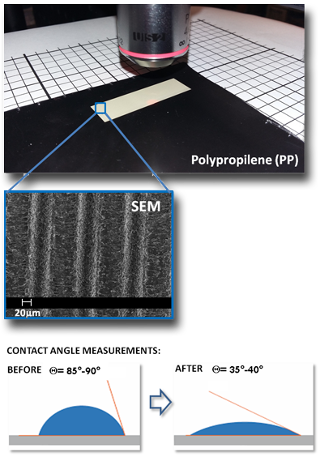
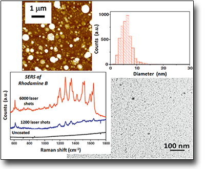
Laser surface treatment of polymers
Polymers are progressively replacing metals and metal alloys in technological applications and there is great interest in physico-chemical treatments for the modification of surface properties. The purpose of these research activities is the modulation of the physical and chemical properties of polymeric surfaces in order to improve their performance in some applications such as solar cells and the automotive sector. Laser treatments are of particular interest to morphologically and chemically modify a polymer. In order to achieve this goal, we use laser sources (al fs or al ns) choosing in the appropriate way the laser parameters such as: pulse energy, laser spot size and distance of the focused laser beam from the sample surface. Processed samples are characterized by scanning electron microscopy (SEM), X-ray diffraction (XRD), u-Raman spectroscopy and wettability measurements. The morphological results obtained so far have shown the formation of periodic structures of micrometric and sub-micrometric dimensions such as to maintain the principal chemical characteristics of the polymer surface but modulating the surface physical properties such as wettability.
- See: A. Guarnaccio et al., Femtosecond Laser Surface Texturing of Polypropylene copolymer for automotive paint applications (in manuscript).
Contact: Ambra Guarnaccio - ambra.guarnaccio@ism.cnr.it
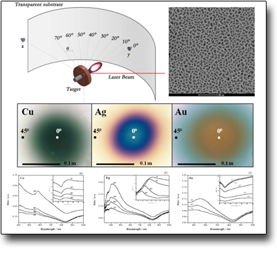
Superficial nanostructuring of materials with various morphologies, also bioinspired and determined by
- use of two fs laser pulses delayed in time in the interval (100 fs-2 ns): 2D-LIPSS;
- linear polarization of the two incident beams (vertical-horizontal) or circular polarization (left-handed-right-handed).
Effects of different morphologies at the nanoscale
- modulable variation of the surface properties of materials (eg chemical-physical, optical, etc.).
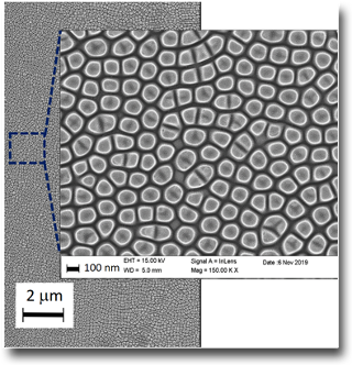
Periodic 2D structures with a pitch of about 80 nm were realized for the first time on monocrystalline diamond surfaces using two linearly polarized and perpendicular to each other ultrashort laser beams (2D-LIPSS) obtained through the development of a Michelson interferometer like experimental set-up and one another optically delayed in the range 100 fs - 50 ps. Through this configuration it has already been shown how it's possible to create periodic surface structures whose pitch ranges from 1/4 to 1/10 of the wavelength of the incident radiation. The extent of the delay between the two pulses in the 2D-LIPSS structuring determines the resulting surface's periodicity. The 2D-LIPSS set up allows to control, in the fs-ps time domain, the interference between the incident laser beam and the induced surface plasmonic polaritons in order to allow, at the nanoscale, the fabrication of 2D surface periodic structures, so as to be able to apply this technique in a versatile way to high band-gap materials by modulating their properties that can be linked to both the dimensional scale and the geometry of the surface's nanostructures generated via 2D-LIPSS.
- See: M. Mastellone et al., submitted, 00 (2020) 00
Applicazioni DiaTHEMA Lab
Contact: Antonio Santagata - antonio.santagata@ism.cnr.it
 English (UK)
  Italiano (Italia)