Pulsed Laser Deposition (PLD) laboratory

Pulsed Laser Deposition (PLD) laboratory

Antonio Morone  - antonio.morone@ism.cnr.it

NanoLAB@TITO

 
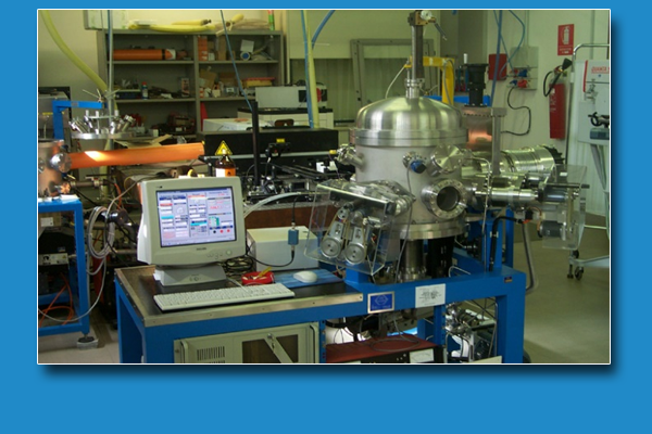
Laser Deposition is a versatile physics technique to obtain functional and advanced materials. It is possible produced thin films, nanostructures and nanoparticles with chemical and physics advanced properties. PLD can be used in biological, organic and inorganic field changing physics laser characteristics. Thin film and nanostructures grow inside high vacuum chamber. X-ray diffraction (Siemens D5000) and Total X-ray Fluorescence (Oxford-Si-Pin) are used, to control chemical and physics properties of news materials. A home-made system for magnetic studies of nanostructured thin films and magnetic nanoparticles by means of magnetooptic Kerr effect (MOKE) in longitudinal geometry is present. The system consists of a photoelastic modulator (PEM), two polarizers, a helium-neon laser, a coil system to generate a magnetic field, a photodiode and the system for data collection and control.
 

TECHNICAL SPECIFICATIONS

PLD

  • Nd-Yag laser (Time= 10 nanosec, Frequency= 10 Hertz)
  • X-Ray diffraction (Siemens D5000)
  • Total X Ray Fluorescence (Oxford-Si-Pin)

MOKE

  • longitudinal geometry
  • He-Ne laser (632 nm)
  • magnetic field 800 G

AVAILABLE TECHNIQUES

  • PLD
  • XRD
  • TXRF
  • Longitudinal MOKE
 

SAMPLE

MOKE

  • thin films

  • nanoparticles deposited and/or grown on substrates that do not have magnetic properties

USE FOR

  • Semiconduttori Organici/Inorganici;

  • Thin films/coatings;

  • Nanoparticelle.


MBE2

III-V MBE 2 growth system MBE2 (III-V)

Paola De Padova - paola.depadova@ism.cnr.it

Carlo Ottaviani  - carlo.ottaviani@ism.cnr.it

Sandro Priori  - sandro.priori@ism.cnr.it

Laboratory IC11

 
In epitaxy the surface is exposed to a gas, for example, Metal (M)/Semiconductor (SC) vapor, which condenses on the surface. In this way the surface becomes a contact place between two solids which is called: interface. The fundamental question in epitaxy is whether the gas atoms adsorbed on the surface wet the surface or form islands. This case occurs as a result of strong forces between adsorbate and surface atoms (at T=0): this is a typical case of adhesion. If the adsorbate-adsorbate interaction is stronger than adsorbate-surface interactions, islands form on the surface, which are termed clusters. Hence, the wetting properties of a “gas” upon a specify surface are the necessary conditions for the epitaxial growth.
 

TECHNICAL SPECIFICATIONS

  • Working pressure ~10-10 mbar mbar  
  • In, Ge, Mn, Ni, Cr, Fe effusion cells;
  • Sb, As, Bi- Surfactants effusion cells;
  • Ag, Zn- Capping Layer effusion cells;
  • DC direct sample heating (RT-1200 °C) and Indirect heating (RT-450 °C ) systems
  • Air-vacuum Fast Load-lock Sample Transfer System;
  • Quartz Microbalance;
  • Ar+ Ion sputtering system;+;
  • O Gas-line;
  • e-- HV variable (0-15) KeV for for RHEED system;
  • e-- HV variabile (0-0.5) KeV for LEED system;
  • AES/SE/REELS spectroscopies; double-pass CMA, e- (HV = 0-5) KeV;ΔE=1.2%PE (UPS/ESCA); ΔE=1.2%Ekin eV (AES);
  • In-situ lock-in  
  • SMOKE system.
  • H-Speed Camera real-time for data diffraction PATTERN acquisition (Image-software-MAC).

AVAILABLE TECHNIQUES

  • Ultra-High Vacuum (UHV) System for Surface Science Investigations:
  • LEED/RHEED/AES/SE
    REELS/SMOKE systems;
  • Chemical composition chemical bonding at surface; work function, molecules hybridization and valence orbitals investigation;  
  • Diffraction pattern  
    from low- and -high e-;  
  • Surface magneto-optics Kerr effect;
  • Analysis of samples in the presence of a gases (O and other);  
  • Heating/cooling (LN) of samples from ~ 80 to 1200 °C during analysis;
  • Clean Semiconductor (SC), Metal (M)-Surfaces reconstruction
  • Epitaxial growth SC/SC, SC/Metal/SC;
  • Homo- and Hetero-structures growth: 1D, 2D and 3D Materials.
 

SAMPLES

  • Sample lateral dimensions: 10 x 5 mm (ideal), 3 x 3 mm (minimal), 10 x 10 mm (maximal);

  • Sample thickness: ideally up to 2 mm (thicker and/or smaller samples also feasible).

USED FOR

  • Fundamental Surface Science study;

  • Artificial Atomic Epitaxial Growth;

  • Discovery of new 1D, 2D and 3D epitaxial SC/SC; M/SC for micro-nanoelectronics and solar cells purposes;

  • Semiconductor/ Microelectronics;

  • Microcircuits;;

  • Ultra-thin Films;

  • Samples Cleaning;
     
  • Thin-film Stability;
     
  • Barrier Layers;
     
  • Lubrication;
     
  • Chemical Industry;
     
  • Coatings/Catalysis.


SQUID Magnetometry

A SQUID (Superconducting Quantum Interference Device) is a very sensitive magnetometer used to measure extremely subtle magnetic fields, based on superconducting loops containing Josephson junctions. The RF sQUID  device acts as a magnetic flux to voltage converter,  detecting  the change of magnetic flux created by mechanically moving the sample through a superconducting second order gradiometer pick-up coil (to suppress the influence of all kinds of external magnetic fields); such change is finally converted to a voltage (VSQUID) profile from which the magnetic moment can be  unfolded by a fit assuming  the dipole approximation. The SQUID magnetometer allows the characterization of magnetic thin films and nanoparticles (in powder or dispersed in liquids) in a wide range of temperature (4K < T < 400K ) and applied field ( Hmax = 5.5 T).

SQUID MPMS XL-5

Seebeck effect measurements

The Seebeck coefficient (S) measurement allows investigating the capability of a material to convert heat to electricity or vice versa. S is a measure of the thermoelectric voltage induced by a temperature difference applied across a material.
The Seebeck coefficient is important for understanding the performance of a material that must be involved in thermoelectric generators or coolers. Moreover, the analysis of the Seebeck coefficient sign allows also to understand the type of the charge carriers involved in the transport of the electrical current induced by the thermal gradient: if S is positive, holes are the main carriers (p-type semiconductors); if S is negative, electrons contribute mainly in the charge diffusion (n-type semiconductors and metals). The generated voltage measurement is performed when applying a thermal gradient between a hot junction and a cold one, and comparing the voltage with the value generated by a reference material operating at the same conditions (e.g. constantan).

SEEBECK

X-Ray Photoconductivity

The photocurrent generated by semiconductors irradiated by an x-ray beam can be a very useful tool for characterizing the materials’ sensitivity to x-ray and response to radiation dose and/or dose-rate. The tool is particularly significant also for evaluating the mobility-lifetime of the semiconductor’s photogenerated charge carriers, that is a measure of its transport capability.
It is based on the measurement of the photocurrent, collected by applying an electric field on the device under test and induced by the interaction with a focusable x-ray beam. The electronic chain for this kind of measurements is particularly sensitive and is made up by a mechanical chopper for x-rays, a trans-impedance amplifier, a lock-in amplifier, and a voltage source.

X-Ray Photoconductivity